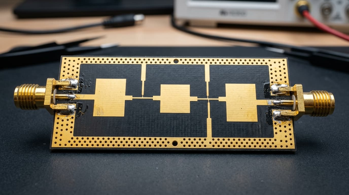
Device Topology & Electromagnetic Behavior
Constructed from alternating sections of very high characteristic impedance (narrow lines acting as series inductors) and very low characteristic impedance (wide lines acting as shunt capacitors). Eliminates 2nd, 3rd, and higher-order harmonics generated by non-linear RF power amplifiers.
Rogers RT/duroid® 5880 (εr = 2.20) for sharpest transition and highest Z_H impedance width ratio.
- Enforce maximum line-width ratio (Z_H / Z_L > 5:1) for optimal lumped component approximation.
- Compensate for step-discontinuity parasitic capacitances at impedance transitions.
Design, 3D EM Simulation & Handoff for Low-Pass Filter (Stepped-Impedance)
We provide turnkey synthesis, multi-frequency full-wave simulation, and fabrication-ready packaging for the Low-Pass Filter (Stepped-Impedance).
1. 3D Full-Wave FEM Modeling
Complete Ansys HFSS 3D CAD modeling with true edge-launch SMA or SMP connectors, via fence stitching, and adaptive mesh refinement down to ΔS < 0.007.
2. Sensitivity & Tolerance Sweeps
Monte Carlo statistical analysis over copper etching tolerances (±15 µm) and substrate permittivity variations to guarantee first-pass high-yield manufacturing.
3. Manufacturing Handoff
Delivery of verified simulation models, parameterized layout geometries, and photolithography-compliant Gerber RS-274X fabrication packages.
More in Filtering & Frequency Selection
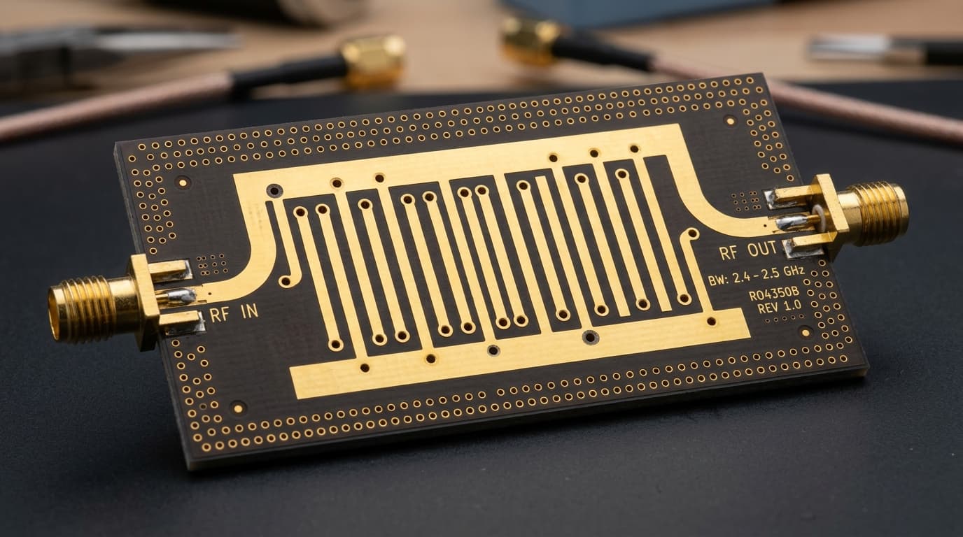
High-Pass Filter (Stub / Quasi-Lumped)
Attenuates low-frequency noise and IF feedthrough while passing high microwave bands.
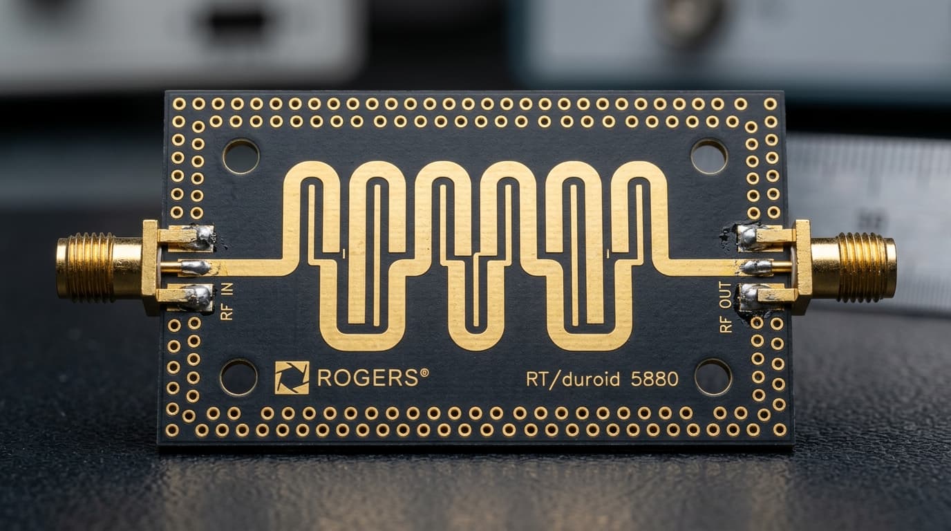
Band-Pass Filter (Coupled-Line / SIW)
High-selectivity bandpass filter with sharp transmission zeros and high Q-factor.
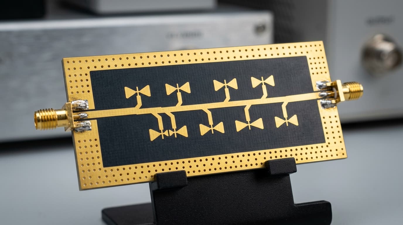
Band-Stop Filter (Notch / Trap)
Deep attenuation notch for eliminating specific high-power interfering carriers.
Initiate Design & 3D EM Simulation Scope for Low-Pass Filter (Stepped-Impedance)
Submit your operational frequency, bandwidth, power handling, and target substrate stackup. Our electromagnetic engineers will deliver a verified feasibility audit within 48 hours.
Initiate Project Scope & NDA
We treat client intellectual property with military-grade rigor. Prior to receiving proprietary disclosure files, patent drafts, or trade secret geometries, we execute standard bilateral NDAs.
Bilateral NDA Standard
Mutual non-disclosure executed before file transmission.
Isolated On-Prem Compute
Simulations run on dedicated air-gapped workstations.
Clean Room Protocol
Full audit trail for IP litigation and patent defense.