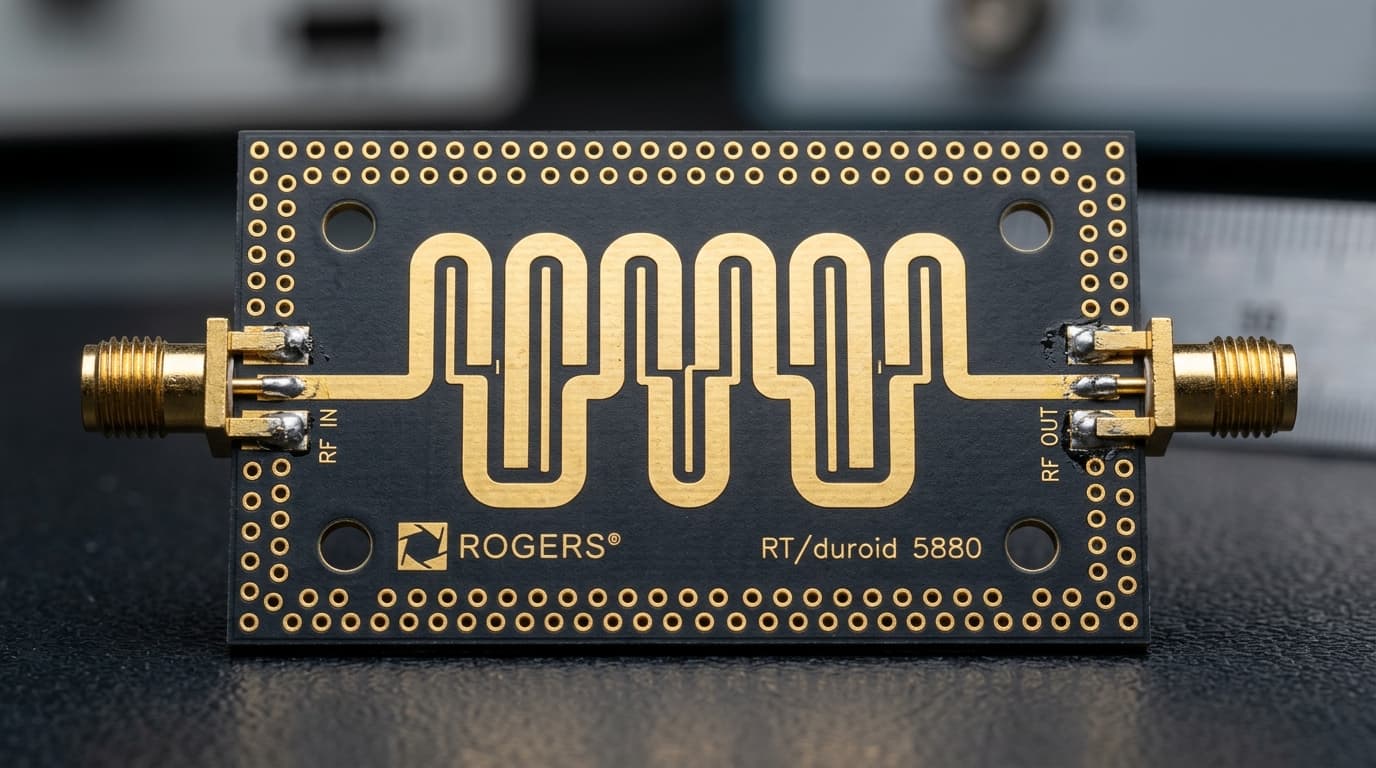
Device Topology & Electromagnetic Behavior
Synthesized using parallel-coupled microstrip resonators, hairpin folds, or Substrate Integrated Waveguide (SIW) resonant cavities. Passes only the intended operating spectrum while deeply rejecting out-of-band spurious responses, image frequencies, and transmitter bleed-through.
Rogers RT/duroid® 5880 (Lowest tan δ = 0.0009) to maximize unloaded Q-factor (Q_u > 350).
- Tight photolithography gap spacing (s down to 75 µm) on end coupling stages.
- Solid via-fence perimeter spacing (pitch p < 2·d) for SIW waveguide enclosure.
Design, 3D EM Simulation & Handoff for Band-Pass Filter (Coupled-Line / SIW)
We provide turnkey synthesis, multi-frequency full-wave simulation, and fabrication-ready packaging for the Band-Pass Filter (Coupled-Line / SIW).
1. 3D Full-Wave FEM Modeling
Complete Ansys HFSS 3D CAD modeling with true edge-launch SMA or SMP connectors, via fence stitching, and adaptive mesh refinement down to ΔS < 0.007.
2. Sensitivity & Tolerance Sweeps
Monte Carlo statistical analysis over copper etching tolerances (±15 µm) and substrate permittivity variations to guarantee first-pass high-yield manufacturing.
3. Manufacturing Handoff
Delivery of verified simulation models, parameterized layout geometries, and photolithography-compliant Gerber RS-274X fabrication packages.
More in Filtering & Frequency Selection
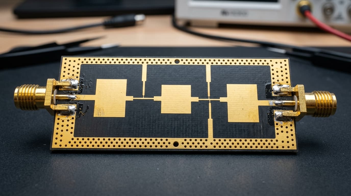
Low-Pass Filter (Stepped-Impedance)
Stepped-impedance microstrip filter for transmitter harmonic suppression.
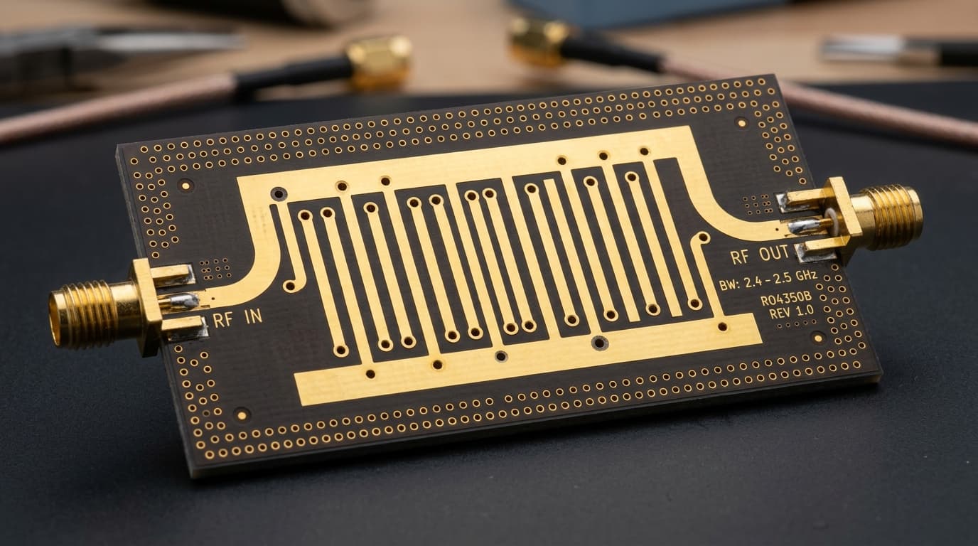
High-Pass Filter (Stub / Quasi-Lumped)
Attenuates low-frequency noise and IF feedthrough while passing high microwave bands.
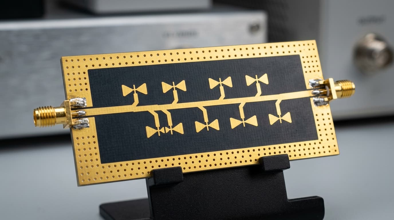
Band-Stop Filter (Notch / Trap)
Deep attenuation notch for eliminating specific high-power interfering carriers.
Initiate Design & 3D EM Simulation Scope for Band-Pass Filter (Coupled-Line / SIW)
Submit your operational frequency, bandwidth, power handling, and target substrate stackup. Our electromagnetic engineers will deliver a verified feasibility audit within 48 hours.
Initiate Project Scope & NDA
We treat client intellectual property with military-grade rigor. Prior to receiving proprietary disclosure files, patent drafts, or trade secret geometries, we execute standard bilateral NDAs.
Bilateral NDA Standard
Mutual non-disclosure executed before file transmission.
Isolated On-Prem Compute
Simulations run on dedicated air-gapped workstations.
Clean Room Protocol
Full audit trail for IP litigation and patent defense.